Why a Busbar's Resistance Rises with Frequency
This is a companion to our cable study, Why Your Charging Cable Gets Warm. That one extracted the parasitics of a thin signal-and-power pair. This one scales up to a power busbar — the flat copper bar that carries hundreds of amps inside an inverter, a switchboard, or a battery pack — and asks a question that trips up a lot of designs: how much does its resistance actually rise once the current is not DC?
The answer is: a lot, and for a reason the handbook cross-section number hides. At DC, current fills the whole conductor and the resistance is simply resistivity times length over area — 34.4 µΩ for this 100 mm², 200 mm bar, which Q3D reproduces to the digit. But an alternating (or switching, or rippled) current does not fill the conductor. It rides in a surface layer whose depth — the skin depth — shrinks as the square root of frequency: about 0.66 mm in copper at 10 kHz and 0.29 mm at 50 kHz. Once that layer is thinner than the bar, the copper in the middle is dead weight, and the resistance climbs.
The skin-effect penalty, measured
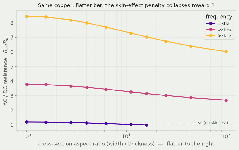
Q3D extracts the full resistance matrix of the bar at each frequency, so the penalty is a direct read, not an estimate. For a square 100 mm² section the AC-to-DC resistance ratio rises past 8.5 by 50 kHz — the current is using only about a tenth of the copper it paid for. That ratio is exactly what a surface-skin argument predicts (the current sits in a perimeter shell one skin depth thick), and the extraction lands on it, which is the check that the numbers are honest.
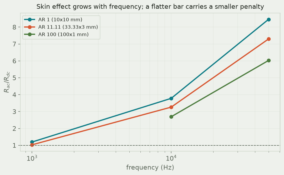
The practical sting is that this happens at frequencies engineers do not always associate with skin effect. A 50 or 60 Hz bus is essentially DC as far as the copper is concerned — the skin depth is many millimeters, larger than the bar. But the moment a bus feeds a switching converter, a motor drive, or anything with current ripple in the kilohertz, the effective resistance is no longer the datasheet DC value, and the extra loss shows up as heat the thermal design did not budget for. That is the gap between a bus that runs at its rated temperature and one that quietly de-rates itself in service.
Why flattening helps — and why it is not a free lunch
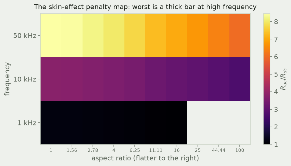
If the current only uses a surface layer, the fix is intuitive: give it more surface for the same copper. A flat wide strip has far more perimeter than a square of the same area, so more of its cross-section lies within a skin depth of a face. That is why, at every frequency in the sweep, the flatter bars carry a lower penalty — the ratio falls from 8.5 toward 6.0 at 50 kHz as the section goes from square to a 100:1 ribbon.
But the improvement is only about 1.4×, not the tenfold you might hope for — and that gap is the useful engineering lesson. A single wide strip does not spread its current evenly along the wide face; the current crowds toward the two edges, so the middle of the face is under-used even though it is near a surface. Widening one strip hits diminishing returns. The way the industry actually beats skin effect in a busbar is to laminate — stack several thin, individually-insulated strips so each is thin enough to be used end-to-end, without the edge crowding of one wide sheet. The sweep shows exactly where a single strip stops paying off and lamination has to take over.
Inductance comes along for free
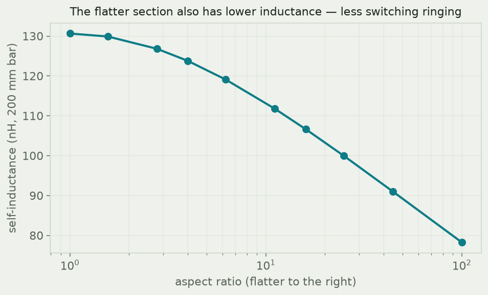
The same extraction returns the bar's self-inductance, and it moves the useful way: the flatter, wider sections have lower inductance (about 78 nH versus 130 nH for the square), because a wide flat conductor stores less magnetic energy per unit current. For a bus feeding fast-switching power devices, that lower inductance means less voltage overshoot and ringing on every switching edge — so the flat section that helps the resistance helps the switching behavior too. Shape is doing double duty.
Put the two together and the design rule for an AC or switching bus is not the DC one. Sizing to a target current density on the cross-section, the way a DC bus is sized, silently under-rates the conductor at frequency: it will run hotter and lose more than the spreadsheet says. The honest procedure is to extract the AC resistance at the real operating frequency, check the temperature rise against that number, and only then decide whether the answer is a flatter bar, a laminated stack, or simply more copper. The value of a sweep like this is that it turns each of those options into a number before any metal is cut.
What the automation did
One busbar was built parametrically and a script swept its cross-section shape across a frequency ladder — 27 converged Ansys Q3D extractions, each returning the DC resistance, the AC resistance with skin effect, and the inductance, one solve at a time with no one at the keyboard. The DC resistance came back at the textbook 34.4 µΩ every time (the built-in sanity check), and the AC ratios traced a clean surface across shape and frequency. Turning a validated single extraction into a design map is the everyday value of scripting the solver — here it turns “busbars have some skin effect” into a chart an engineer can size a bus from.
What this model does and does not cover
Sizing a bus, a cable, or a laminated stack that has to carry real current at real frequency? The DC number on the datasheet is the optimistic one; the AC penalty is where the heat and the loss actually live, and it is a direct extraction, not a guess. We do this in Ansys Q3D, Maxwell and Icepak. Rand Simulation — innovation through insight.