Can You Thread a Laser Through a Needle?
The Scale of the Problem
A single-mode fiber carries light in a core about nine microns across. The waveguides on a silicon photonic chip are 500 × 220 nm — a cross-section roughly 500 times smaller in area, buried at the edge of a die. Between them sits the least glamorous and most expensive problem in photonics: getting the light from one into the other. Industry veterans put packaging and assembly at up to 80% of the cost of a photonic component, and the single largest reason is that this alignment cannot be done by ordinary pick-and-place — the tolerances are submicron, so every part goes through slow active alignment, wiggling the fiber while watching the light meter.
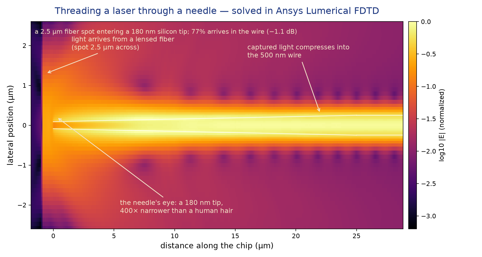
The standard trick for closing the size gap is beautiful and counterintuitive: make the waveguide smaller. Narrow a silicon wire down to a tip one or two hundred nanometers wide and the mode can no longer fit inside the silicon; it swells out into the cladding into a micron-scale spot that a focused fiber beam can actually match. Then taper the tip back up to full width over tens of microns, and the swollen mode is adiabatically squeezed into the wire. The tip is the needle's eye — and paradoxically, the smaller the silicon, the bigger the target.
Shaping the Needle
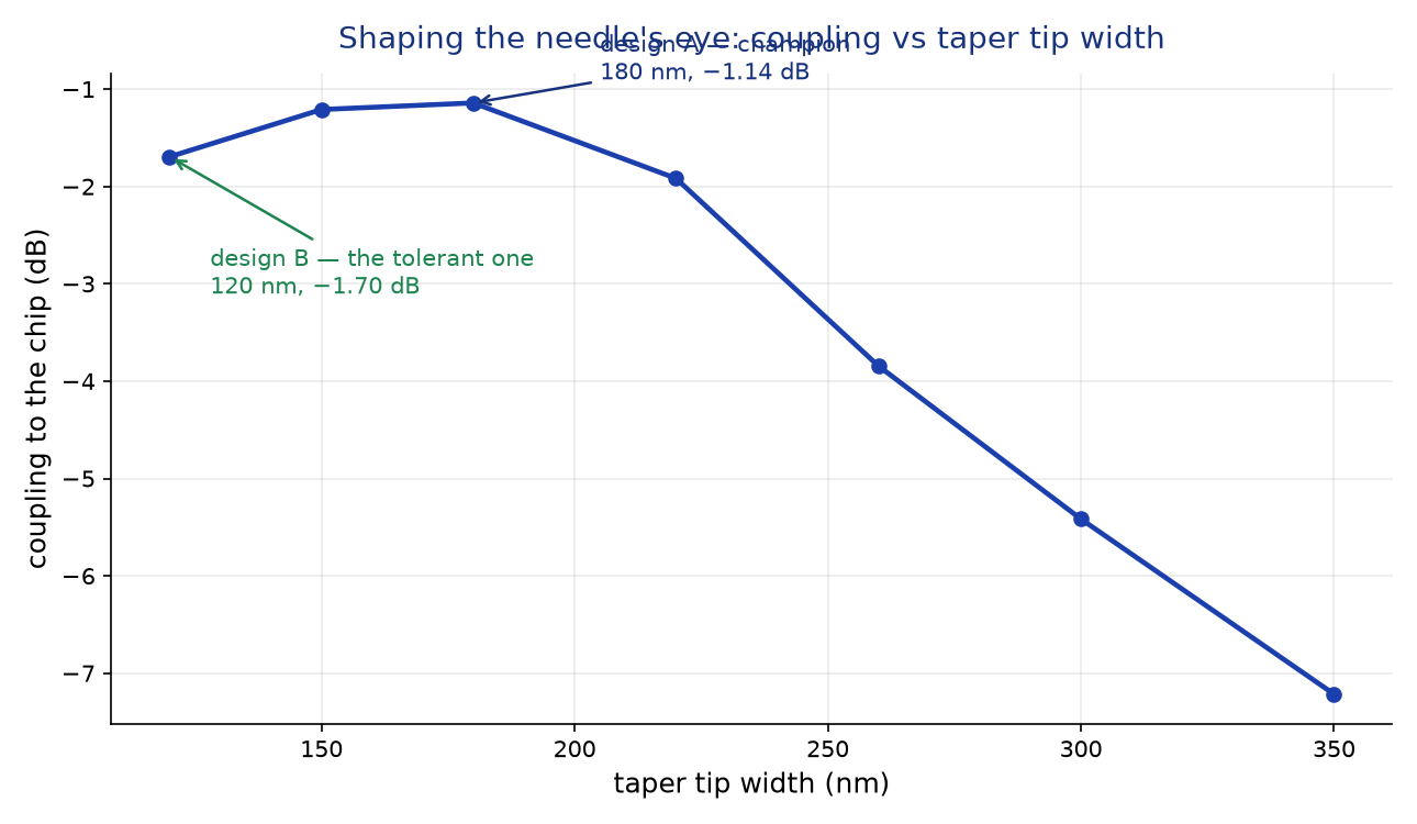
We built the coupler in Ansys Lumerical 3D FDTD: a 220 nm SOI platform, oxide-clad, with a linear inverse taper running from a swept tip width up to a 500 nm wire, driven by a lensed-fiber Gaussian spot 2.5 µm across — the sharpest common packaging fiber. The figure of merit is honest end-to-end coupling: power arriving in the fundamental mode of the output wire, verified against a co-located raw power monitor (they agree within 1%, confirming nothing is sneaking through in higher-order modes).
Then We Missed on Purpose
A coupler's datasheet number assumes perfect aim. Real packaging machines drift, epoxy shrinks, temperature cycles walk the fiber. So we swept the miss: lateral offsets to 2 µm, vertical offsets, facet tilt to 4°, and ±20 nm of lithography error on the tip itself — for both designs.
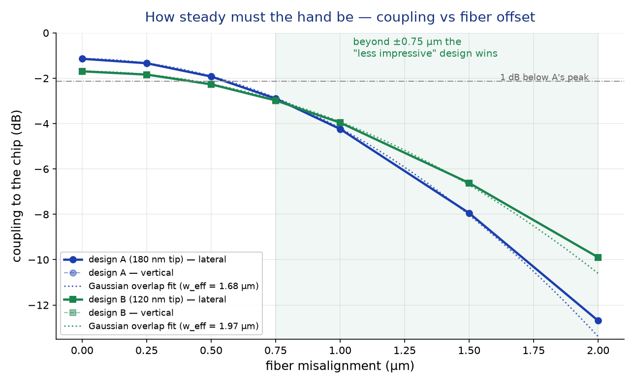
The crossover is the finding. Design A is only the champion inside a ±0.75 µm circle of aim. If your assembly process genuinely holds half a micron for the life of the part, buy the champion. If it holds a micron on a bad day — thermal cycling, epoxy creep, a Friday-afternoon bond — the blunter tip is worth more than its spec-sheet number every day after the first. The tilt sweeps add the reassuring counterpoint: at 4° both designs lose only a quarter of a decibel, because a tilted beam still mostly overlaps a spot this small. Aim matters; attitude barely does.
The fabrication sweep produced this study's honest wrinkle: the champion is actually the fab-tolerant one. Its ±20 nm lithography window moves coupling by only 0.27 dB, while the 120 nm design swings 0.81 dB — and an over-etched “error” on the blunter tip actually improves it, because 140 nm is a step back toward the sweet spot. Robustness is not one number: this coupler asks you to choose which error you fear more — the packaging machine's, or the fab's.
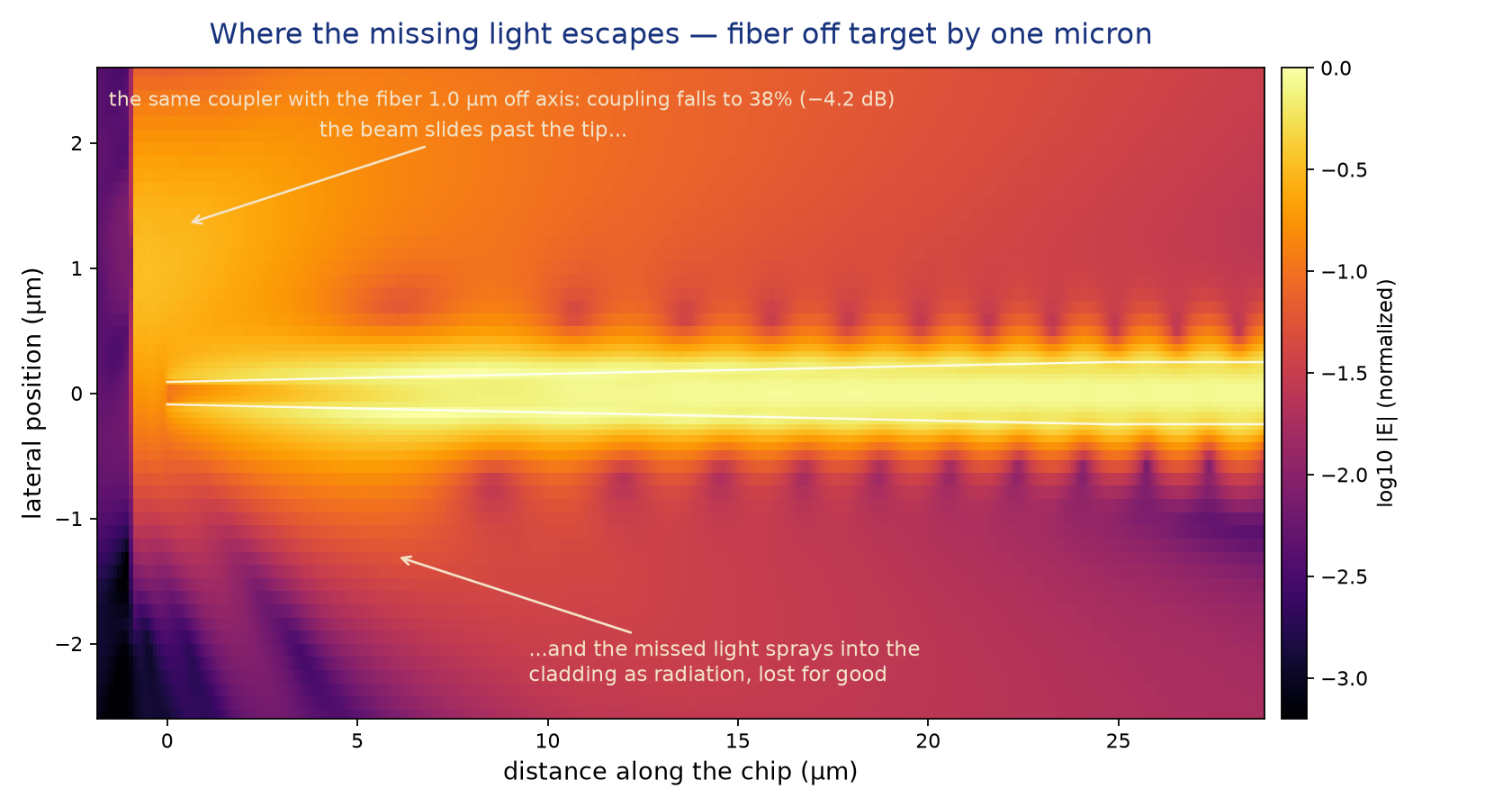
Where the Missing Light Goes
The Numbers Against the Literature
Every headline number here lands on a published anchor. Our −1.1 dB champion sits between the −1.25 dB measured for a 2.5 µm lensed fiber on a comparable platform and the −0.25 dB research-record couplers with 300 µm adiabatic tapers; foundry PDKs quote 1.5–2 dB per facet as typical. The submicron 1-dB tolerance is the canonical published figure for small-spot edge couplers — and it is exactly why the industry also builds grating couplers (±2 µm tolerance, at other costs) and why relaxed-tolerance edge couplers are a live research area for co-packaged optics. And the rolloff itself needed no simulation to predict — the Gaussian overlap integral drew the same curves — but the crossover between two real designs, with fabrication error folded in, is the kind of decision-grade result only the full-wave solve delivers.
Choosing a coupler, a packaging process, or an alignment budget for a photonic product? The datasheet number is the easy part — the money is in how the design behaves when the aim is off by the width of a virus. We run fiber-to-chip coupling, tolerance, and yield studies in Ansys Lumerical, geometry through misalignment budget. Rand Simulation — innovation through insight.