A Lens Thinner Than a Human Hair, and a Focus That Will Not Stay Put
A thermal camera works in a band of light your eye has no cells for: 8 to 12 micrometers, the wavelengths a warm body glows at. The lenses that gather it are thick, heavy and made of germanium. Here is the alternative — a flat sheet of silicon pillars 11.5 micrometers thick, thinner than a human hair, that brings that light to a focus 50 micrometers across. It works beautifully. It just refuses to put every color in the same place.
A lens made of obstacles rather than thickness
An ordinary lens bends light by being thick in the middle. Light crossing the fat center is slowed more than light skimming the thin edge, the wavefront tips inward, and the beam converges. Everything about that is geometry: the glass has to physically be the shape of the delay it imposes.
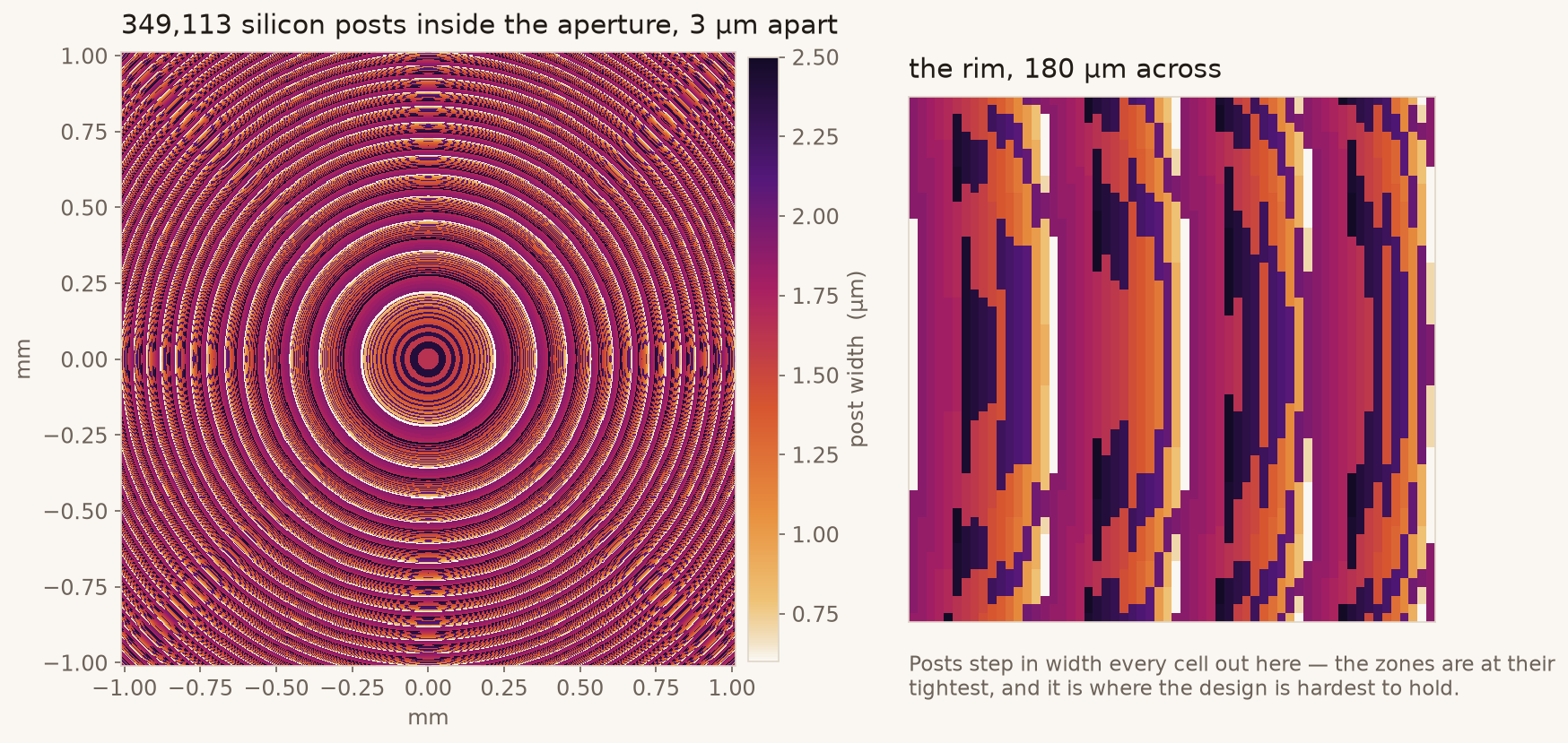
A metalens throws that away. Instead of varying thickness, it covers a flat surface with pillars far smaller than the wavelength — here, silicon posts 10 µm tall on a 3 µm grid, each between 0.6 and 2.5 µm wide. Light passing a fat pillar is held up more than light passing a thin one, because a fat pillar behaves like a stubbier, higher-index waveguide. Choose the width at each point and you dial in the delay you want, point by point, with no thickness anywhere.
The delay a good lens needs is the hyperbolic phase: enough extra hold-up at the center that a ray from the rim and a ray from the middle reach the focus together. At 10 µm over a 2 mm aperture at f = 4 mm that is 12.3 full waves from center to edge, and no pillar can hold light back that far. But phase repeats every 2π — 12.3 waves is optically indistinguishable from 0.3 — so the design is wrapped into rings, twelve across the radius and twenty-five out to the corner. It is a Fresnel lens, at a thousandth of the scale.
Thirty-three pillars, measured one at a time
None of that works unless you know precisely what each pillar does, and that is not something to be assumed. Each candidate width gets its own 3D FDTD solve in Ansys Lumerical: one pillar inside an infinite array of identical neighbors, illuminated at normal incidence, with the transmitted field recorded as a complex number — a magnitude and a phase — at 201 wavelengths across the band.
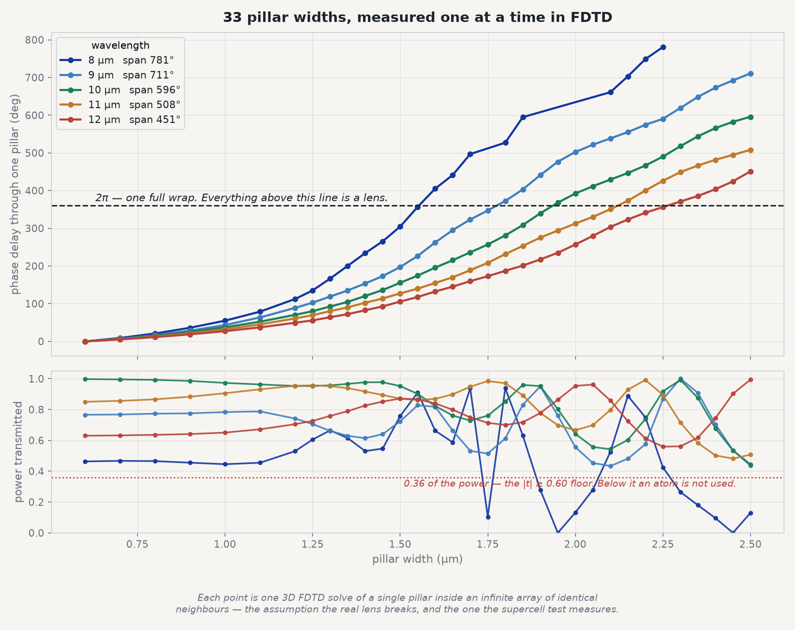
Two things have to be true for a library to be usable, and both are read straight off that chart. The phase has to cover a full 2π, or there will be delays the lens needs and cannot build — at 10 µm the span is 596°, so there is room to spare. And each chosen pillar has to actually transmit; anything passing less than 36 % of the power is rejected outright, which is what removes the resonant widths where the pillar rings like a bell and gives the light back where it came from. Thirty-three widths survive both tests.
Inside the model
Each pillar is solved in Ansys Lumerical FDTD as a full 3D unit cell: one silicon post, refractive index 3.4178, standing 10 µm tall on a 1.463 µm membrane, with Bloch boundaries on all four sides to impose the infinite array and perfectly matched layers above and below. A plane wave enters from beneath, a field monitor a few micrometers above the post records the transmitted amplitude and phase, and the run is broadband — one solve returns all 201 wavelengths at once, so the dispersion is measured rather than interpolated between design points. Twenty-nine widths were solved in the first pass and four more added to close gaps in the phase coverage.
The finished lens goes to Ansys Zemax OpticStudio as a Grid Phase surface on a 675 × 675 grid, where the focal plane is found by sweeping the image distance for minimum spot. One setting there matters more than it looks: the interpolator must be linear. The default spline fits a curve through what is deliberately a staircase and overshoots at every step — 193 µm of spot against 60 µm for linear, on a lens whose Airy radius is 25 µm. The hero comes from a third calculation again: an angular spectrum of plane waves, exact for a scalar field with no paraxial approximation, run on the measured pupil.
Those thirty-three are then laid down across the aperture, each cell taking the pillar whose measured phase comes closest to the delay the design wants there. The result is a real, buildable object: 349,113 pillars inside the 2 mm aperture, each one an entry from a measured table.
Is it right? A lens that must not focus, and two sums that must agree
A focusing result is the easiest kind to fake, because a rig that quietly assumes a lens will find one. So the first thing through it was a lens that must not work: the same Grid Phase surface, attached exactly as before, carrying zero everywhere. A flat pupil has no business focusing, and this one does not — a 707 µm blur where the real lens gives a sub-micron spot. That control ran before any result was looked at.
The second check is harder to fool because it uses different physics on the same file. The focal positions were found twice: once by ray tracing in OpticStudio, which follows the local slope of the phase, and once by fitting a reference sphere to the wavefront, which never traces a ray at all. Those two have no reason to agree unless both are right. Across all five wavelengths the worst disagreement is 0.17 %.
That pairing also settles which number to quote. At 10 µm the wavefront is 0.0145 waves RMS — essentially perfect — while the ray-traced spot radius reads 43 µm. Both are correct and they measure different things: the lens is a staircase, so its amplitude error is tiny but its local slope error is not, and a ray follows the slope. Below the Airy disc a geometric spot radius has no physical meaning, so the wavefront is the metric here and the ray trace keeps the job it does well — finding the focal plane.
Where each color actually lands
The focal sweep is not a defect of this particular design — it is what a flat lens is, and the reason runs opposite to the intuition glass gives you.
A pillar imposes a fixed phase. It does not know what color is passing through it — it is a piece of silicon of a particular size, and the delay it applies is the delay it applies. But the angle light is deflected through depends on that phase gradient measured in wavelengths, so longer light, with fewer wavelengths per millimeter, is bent further by the same structure. Longer wavelength, stronger bending, shorter focal length. The focus should march as f₀·λ₀/λ, and it does.
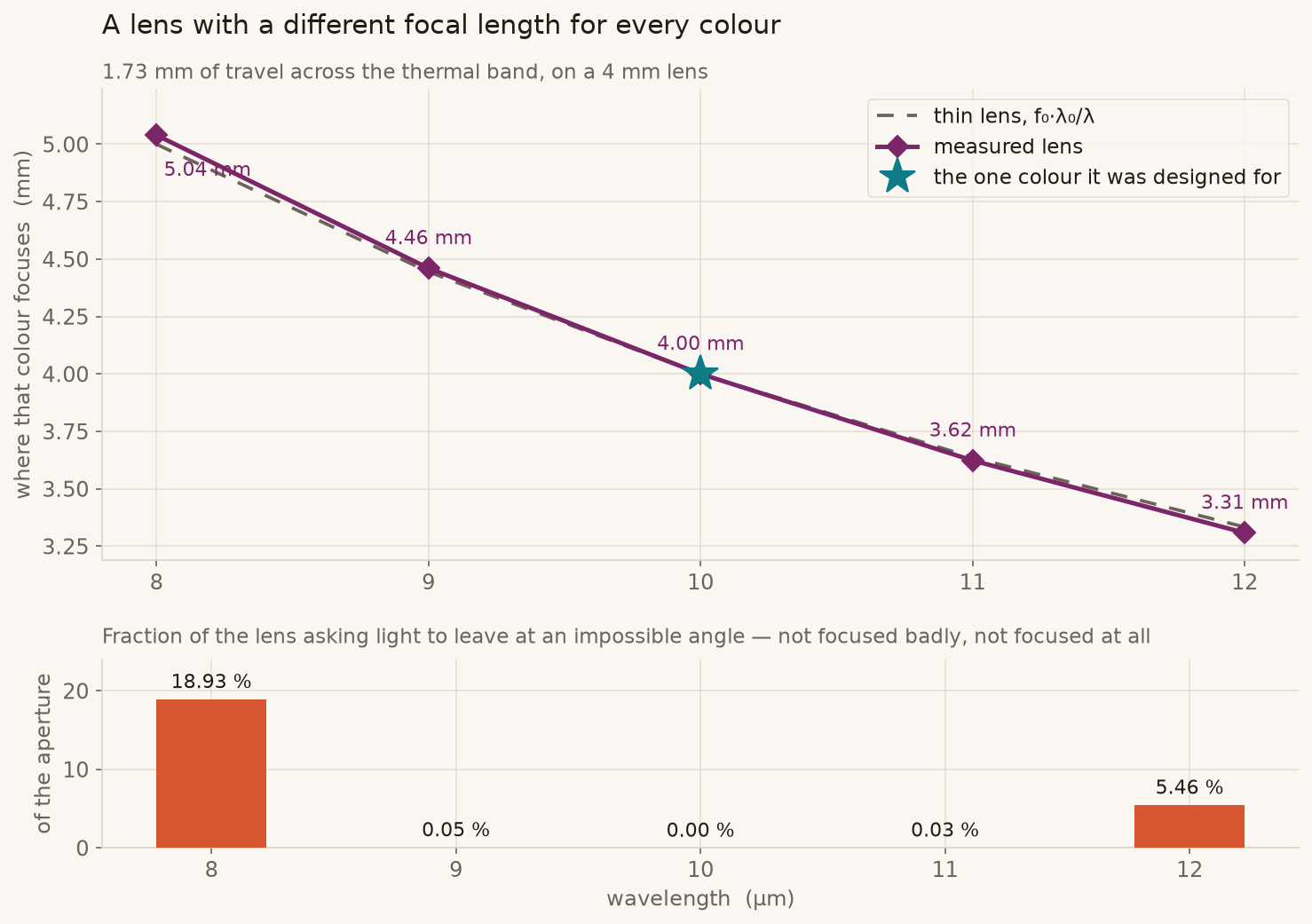
Notice that this is exactly backwards from a glass lens, where blue focuses closer than red. A metalens is chromatic in the opposite direction, and violently so: over the thermal band this focus moves 1.73 mm, which is 43 % of its own focal length. Refractive lenses are chromatic in the hundredths.
The bottom panel is a limit worth naming rather than hiding. A phase profile can only steer light so far: past a certain local gradient, the deflection it demands corresponds to an angle whose sine exceeds one, which is not a steep ray but an impossible one. That light goes into evanescent and high-angle channels and never reaches the focus. At the design wavelength no part of the aperture is in that state. At 8 µm nearly nineteen percent of it is.
Only one thing is to blame
So the lens falls apart away from its design color. The interesting question is which part of the design does it — and there are three plausible suspects. The wrapping into zones, which throws away the smooth profile. The quantization, because there are only thirty-three pillars to choose from and the delay you want is rarely one of them. And the pillars' own dispersion, the fact that a fixed piece of silicon does not hold every color back by the same amount.
Those can be separated by building three lenses that differ by exactly one ingredient each and putting all three through the same Ansys Zemax OpticStudio rig: a perfect continuous phase; the same design snapped to the thirty-three real pillar phases; and finally those pillars carrying the dispersion the FDTD actually measured.
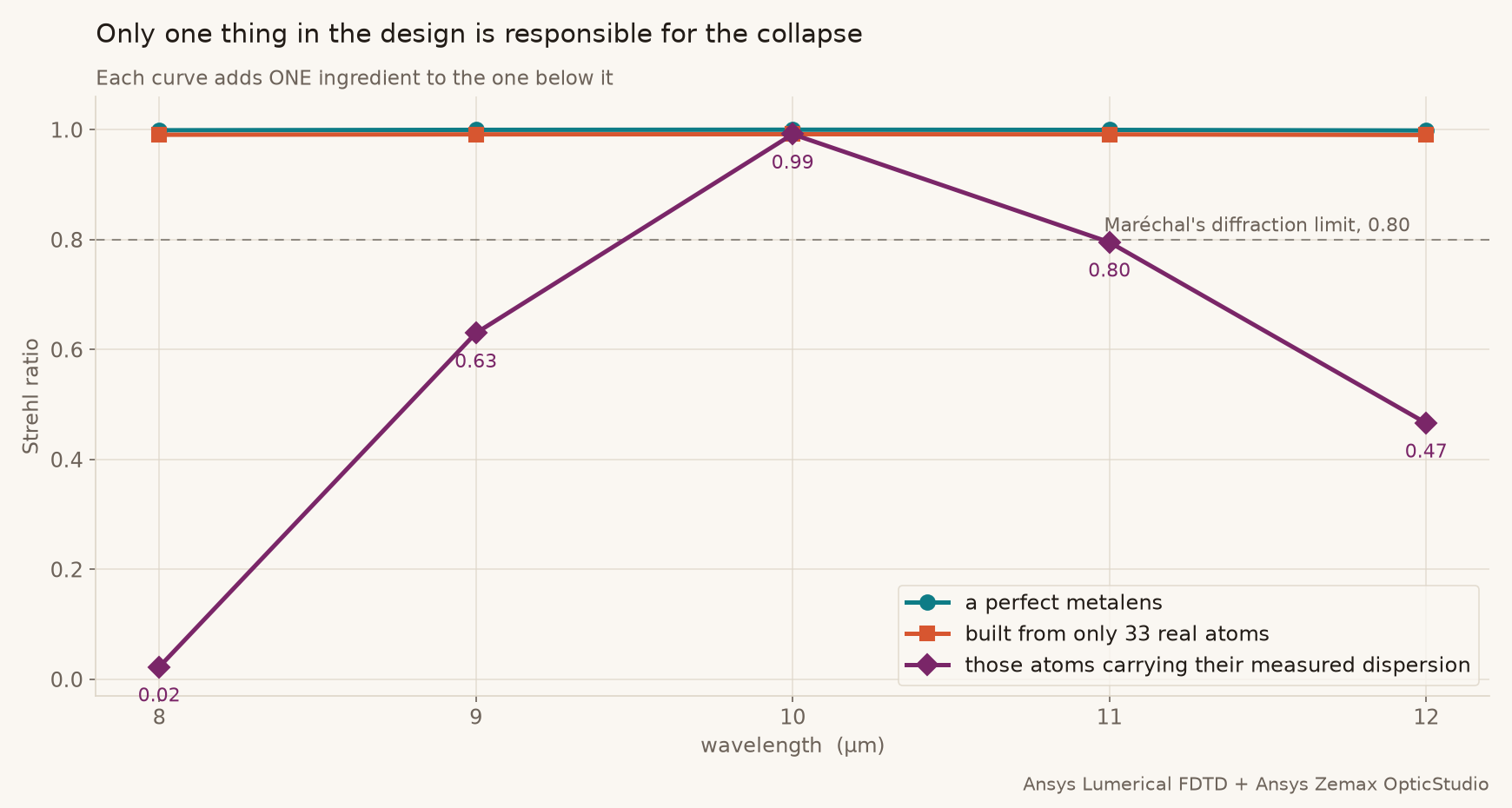
The answer is unambiguous, and it is not the suspect most people would name. Having only thirty-three pillars to choose from is nearly free — it costs 0.8 % of Strehl, and it costs the same 0.8 % at every wavelength, which is the signature of an error that does not care about color. Wrapping costs nothing measurable at all. The entire collapse is dispersion: the pillars near the middle of the table drift by one amount as the color changes, the pillars near the ends drift by another, and a phase profile assembled from both comes apart.
That matters for what you would do about it. A finer library will not help; you could have three hundred and thirty pillars instead of thirty-three and recover less than a percent. What helps is pillars chosen so their drift matches as well as their phase — which is precisely what the achromatic metalens literature does, at the cost of needing a much richer geometry than a simple square post, and usually a smaller aperture.
What a flat lens is actually for
Read the Strehl curve as a specification rather than a disappointment and the application picks itself. Between about 9.5 and 11 µm this lens is at or near the diffraction limit, in a package thinner than a hair, at a mass a ground germanium element cannot approach. Gas sensing lives there — ammonia, sulfur hexafluoride and the fluorinated refrigerants all absorb inside that window — and so does the 10.6 µm carbon-dioxide laser line, almost exactly at the design wavelength.
What this lens cannot do is be a thermal camera objective, because a camera does care: it collects the whole 8 to 12 µm band at once, and a focus that moves 1.73 mm across that band puts most of the light somewhere other than the sensor. That is not a flaw in the fabrication or the model. It is the physics of a flat optic, and it is measurable before anything is etched.
Which is the general point. The chromatic sweep, the quantization cost, the fraction of the aperture that stops working at the band edge — all of it comes out of a pillar library and a diffraction calculation, on a design that exists only as a table of widths. The expensive way to learn that a flat lens is too chromatic for your band is to make one.
Have a flat optic, a diffractive element or a metasurface where you need to know what it does across a real band, not just at one line? The same Ansys workflow behind this lens — a pillar library measured one solve at a time in Lumerical FDTD, assembled into a physical design, then put through OpticStudio and an independent diffraction propagation that have to agree before either is believed — is how Rand Simulation turns "it should focus" into a Strehl number at every wavelength you care about, before a mask is written. That is innovation through insight.