
Why Your PCB Browns Out — and Why a Fistful of Tiny Capacitors Fixes It
Look closely at the motherboard around a CPU socket, or the die-side of a modern GPU, and you will see a swarm of tiny rectangular capacitors — dozens, sometimes hundreds — crowded as close to the chip as the layout allows. They are not decoration and they are not an afterthought. They are there because a modern processor can slam its current draw from a few amps to tens of amps in nanoseconds, and when it does, the voltage on the power rail momentarily sags. Sag too far and the chip glitches, resets, or throttles — a brownout, on a circuit board. We built a small power-delivery network in Ansys SIwave and measured exactly how far the rail sags, at every frequency, and watched each capacitor we added claw the sag back down.
The physics: a power rail is an impedance, and the chip is the current source
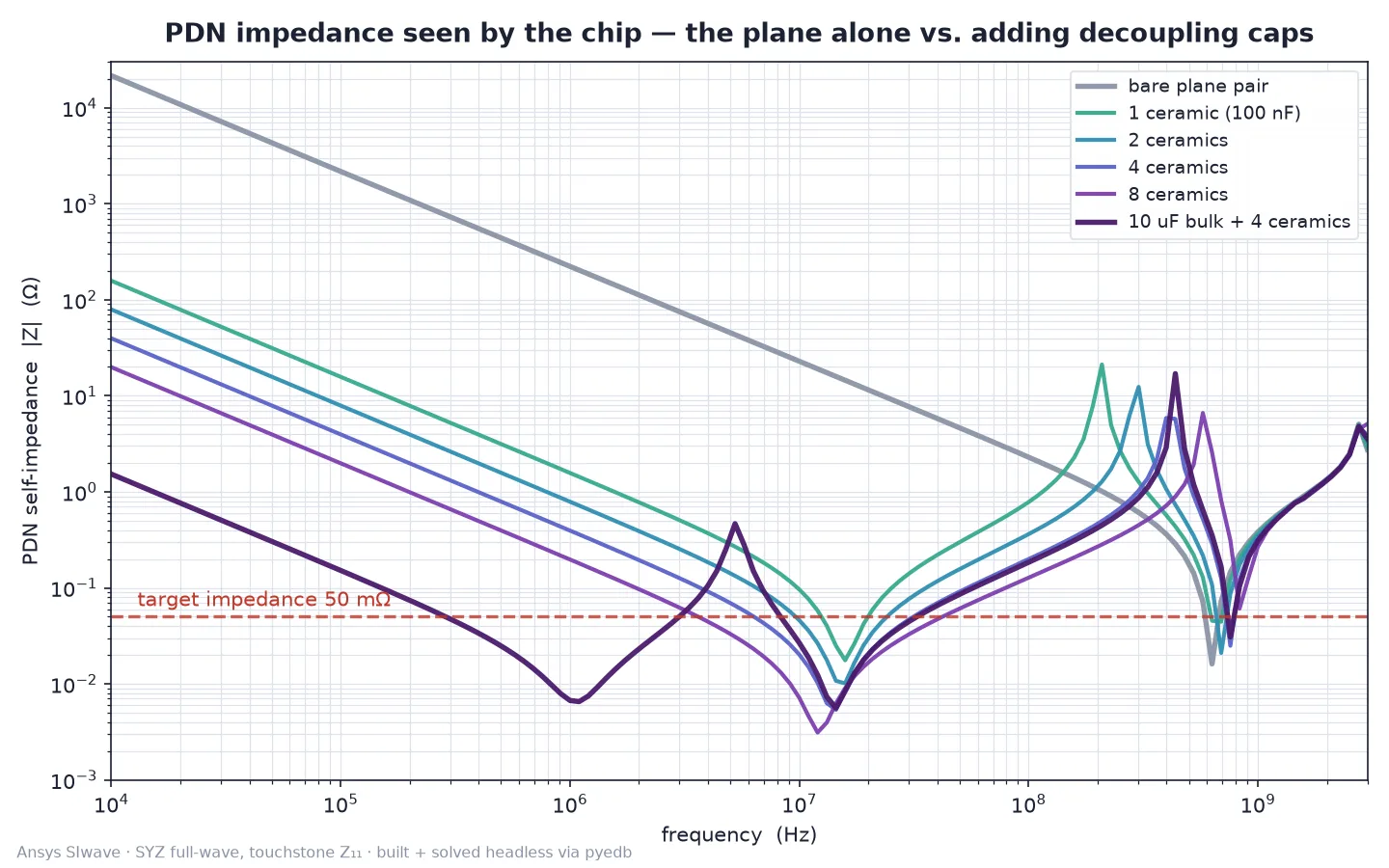
Engineers are trained to think of a power rail as a node — “1.0 volts” — but a chip does not see a node. It sees an impedance, Z(f), looking back into everything that feeds it: the voltage regulator, the copper planes, the vias, and every capacitor along the way. Ohm’s law does the rest. When the chip’s current changes by ΔI at some frequency, the rail voltage moves by ΔV = Z(f) × ΔI. Keep Z low across every frequency the chip can excite and the rail stays put; let Z spike anywhere and the rail dips there. That is the whole game of power integrity, and it is why designers set a target impedance — a flat ceiling Z(f) must live under from DC to hundreds of megahertz, computed as the allowed ripple divided by the transient current step: Ztarget = ΔV/ΔI. For this coupon we set 50 mΩ — a 50 mV allowance (5% of the 1.0 V rail) against a 1 A step. That is a deliberately gentle budget chosen so this small board’s capacitor staircase is legible on one chart; a production rail feeding the full 25 A chip, budgeted for tens-of-amps swings, would demand a ceiling in the low milliohms — same logic, lower line.
The bare board is already a capacitor: two copper planes separated by a thin dielectric are a parallel-plate cap, and a capacitor’s impedance falls with frequency. That is backwards from what a chip needs. At low frequency the plane pair is a minuscule fraction of a nanofarad, so its impedance is huge — kilo-ohms — and useless. This is the gap the capacitors fill. A decoupling cap is a local reservoir of charge sitting microns from the chip; when the chip gulps current faster than the distant regulator can respond, the cap supplies it and holds the rail up. Add a capacitor and you pour capacitance into the network, dragging the impedance down exactly where the chip lives.
Inside the model
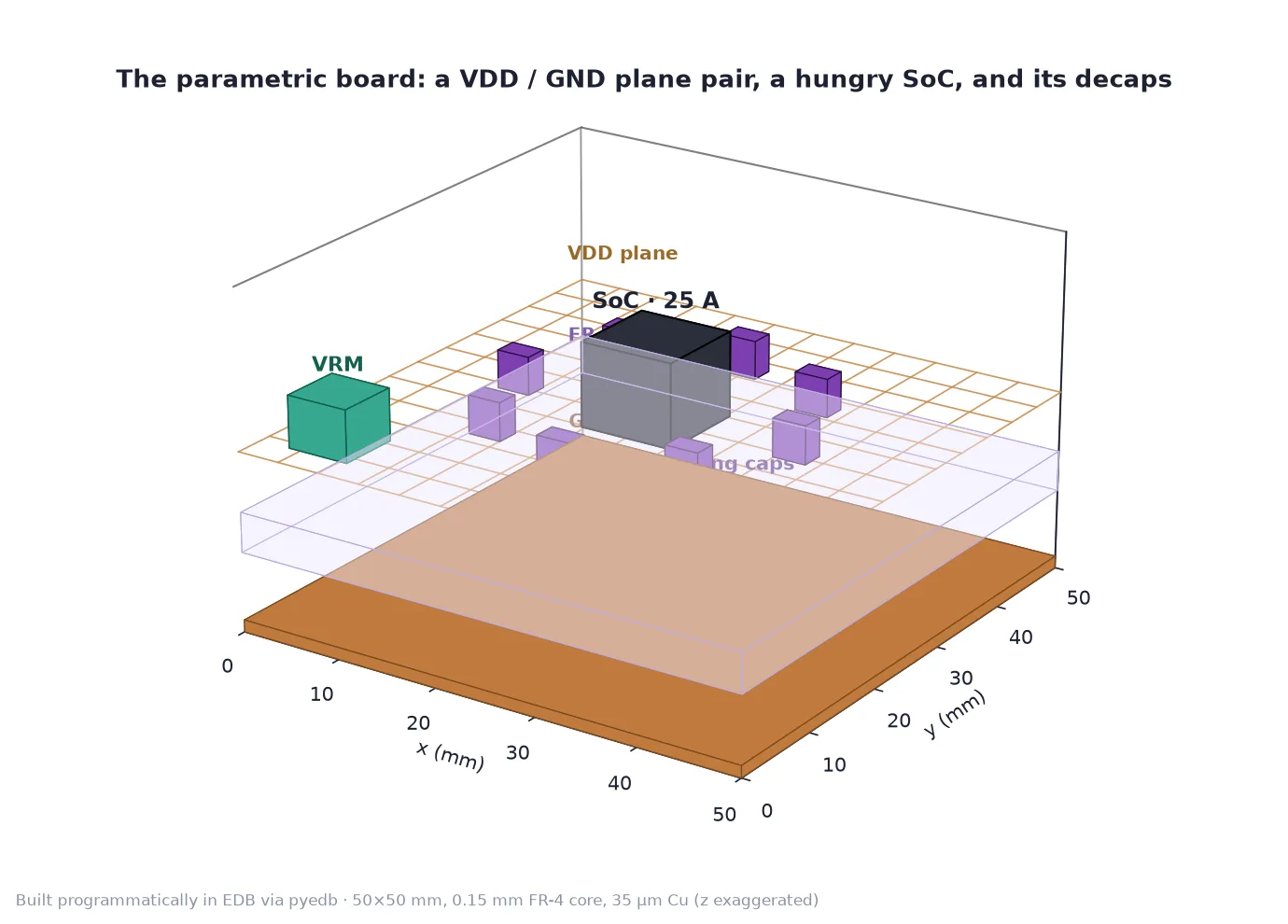
The board is deliberately small so every number is traceable: a 50 × 50 mm square with a VDD plane over a GND plane, separated by a 0.15 mm FR-4 core (εr = 4.4), both planes 35 µm (1 oz) copper. A hungry SoC sits at the center; its decoupling capacitors ring it a few millimeters out, each mounted on its own pair of plated through-vias. The capacitors are real RLC models — a 100 nF ceramic carries 0.8 nH of mounting inductance and 15 mΩ of series resistance; the bulk cap is 10 µF with 2 nH and 5 mΩ. The entire stack-up, planes, vias, components, and ports were built programmatically in EDB with pyedb — no GUI — and solved by Ansys SIwave 2026 R1, its full-wave SYZ engine extracting the one-port scattering response at the chip and exporting a Touchstone file. The self-impedance is Z11 = Z0(1 + S11)/(1 − S11), swept from 10 kHz to 3 GHz. Six populations were solved — bare plane; 1, 2, 4, and 8 ceramics; and a bulk-plus-ceramic mix.
Is it right? Three hand-calcs the solver was not told about
The pretty curves are only worth trusting if the physics behind them is predictable, so we checked SIwave against pencil-and-paper on three independent fronts. First, the plane capacitance. A parallel-plate cap is C = ε0εrA/d; for this board that is 0.649 nF. Reading the capacitance straight off the bare-plane impedance at 10 kHz gives 0.735 nF — 13% higher, which is exactly the sign and size you expect once fringing fields past the plane edges are included. Second, the parallel-capacitor rule. N identical caps in parallel should give N times the capacitance and therefore 1/N the impedance; the solved 100 kHz impedances for 1, 2, 4, 8 ceramics were 15.80, 7.93, 3.97, 1.99 Ω — matching the ideal 1/(2πfNC) to better than 1%. Third, the self-resonance. Every real capacitor stops being a capacitor above its self-resonant frequency f = 1/(2π√(LC)); for the 100 nF/0.8 nH ceramic that is 17.8 MHz. SIwave put the impedance minimum at 15.9 MHz — slightly lower because the solver includes the extra inductance of the mounting vias and the spreading path (it implies ~1.0 nH of total loop inductance versus the 0.8 nH we specified). Three checks, three matches, none of them handed to the solver.
That self-resonance is also the key to the anti-resonance peaks in the figures. Below its resonance a cap is capacitive; above it, the cap goes inductive. When an inductance meets a capacitance in parallel, the two form an LC tank — and a parallel tank has high impedance at its resonance. At 437 MHz, every capacitor on this board is far above its own self-resonance, so the whole decap bank has collapsed into a small inductance: eight mounted ceramics in parallel present roughly an eighth of the ~1.0 nH loop each carries — with the bulk cap in parallel and the plane’s spreading path to the chip port, call it ~0.2 nH. The only thing still capacitive up there is the plane pair itself, and that is the tank: 1/(2π√(0.2 nH × 0.65–0.74 nF)) spans 415–442 MHz, bracketing the solved 17 Ω spike at 437 MHz. (The tank intuition reaches for first — the bulk cap’s 2 nH going inductive against the ceramics’ combined 0.8 µF — resonates near 4 MHz by the same formula, where the parts’ ESR damps it to a gentle bump; it is not this peak. A spike like this one belongs to every decap-populated board: it is the decap bank handing the job back to the planes.) This is why you cannot just bolt on one giant capacitor and call it done: real PDN design is a staircase of capacitor values, each covering a band, chosen so nobody’s anti-resonance lands where the chip is loud.
The other half of brownout: DC IR-drop
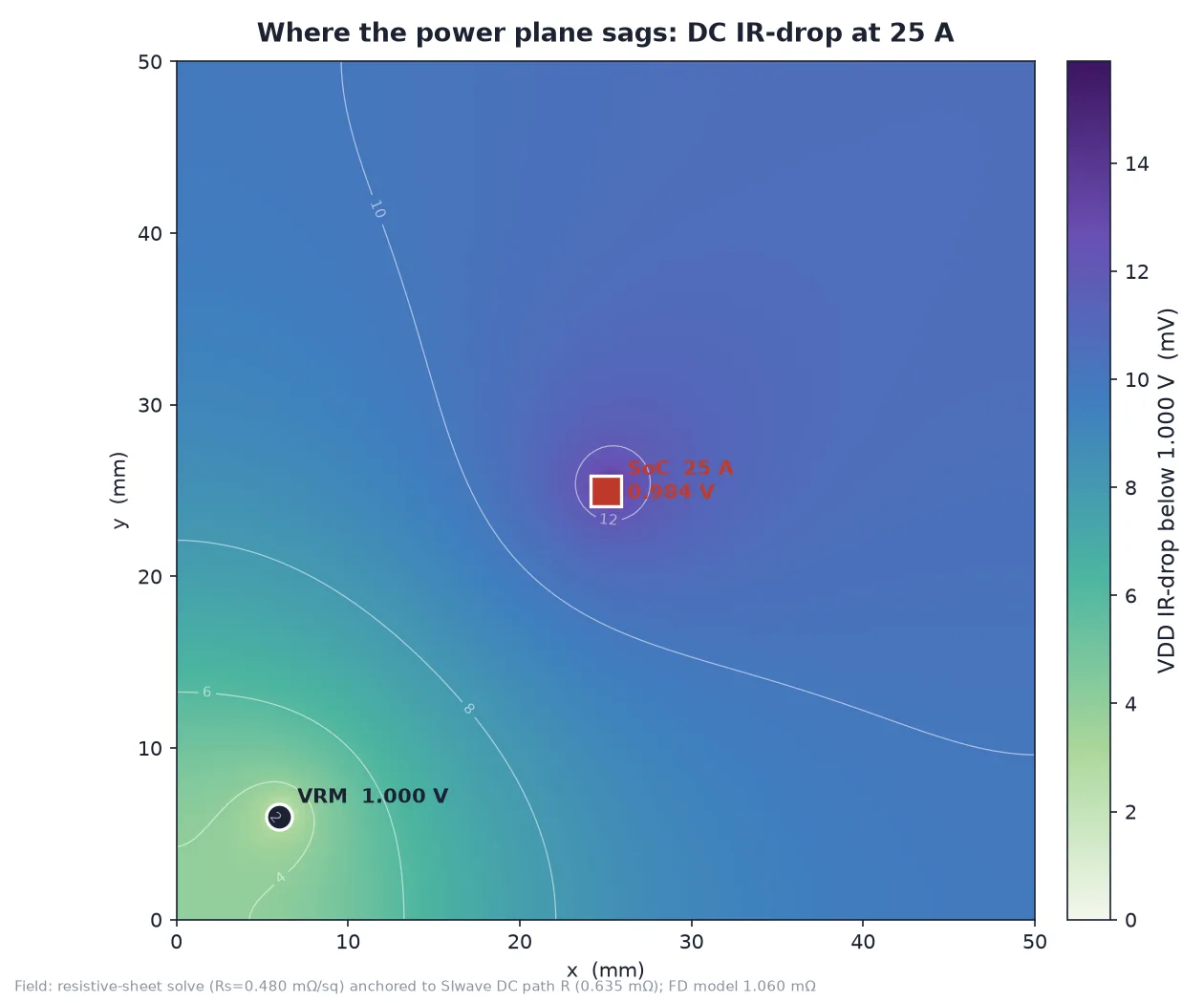
Impedance is the dynamic story; there is a static one too. Even holding a steady current, the copper plane has resistance, so the voltage the chip receives is lower than the voltage the regulator delivers — a plain IR-drop. Our DC solve pushed 25 A from a corner regulator to the center SoC and measured a plane path resistance of 0.64 mΩ on VDD and 0.62 mΩ on the ground return — consistent with the copper’s 0.48 mΩ-per-square sheet resistance and the spreading geometry. That is a 31 mV round-trip droop, 3.1% of the 1.0 V rail, before a single transient even happens. The map below shows where the plane sags worst: a smooth gradient from the regulator to the chip, deepest right under the SoC.
Why it matters: the swarm of caps is a designed frequency response
Next time you see a processor surrounded by a moat of little capacitors, you are looking at a hand-tuned impedance curve. The big bulk caps handle the slow, deep current swings; the mid-size ceramics cover the megahertz; the smallest, closest caps — and eventually the capacitance built onto the silicon itself — handle the fastest edges the planes can no longer keep up with. Each is placed and valued to hold the rail’s impedance under target across the whole band the chip can excite, and to keep anyone’s anti-resonance out of the danger zone. Get it wrong and the symptoms are maddeningly intermittent: a GPU that crashes only under a specific load, a CPU that throttles when it should sprint, a radio whose noise floor rises when the digital core switches. Get it right and the chip never knows the regulator is centimeters and microseconds away.
This is the same workflow — build the plane stack, model the decoupling, solve the impedance from DC to gigahertz, and check the DC drop — that decides whether a board spin will be stable at full load or a field-return waiting to happen. Doing it before the board is fabricated is orders of magnitude cheaper than probing a rail droop on a bench and guessing which capacitor to move.
Need a power-delivery network checked — target impedance, decoupling strategy, or DC IR-drop — before you commit a board to fab? The same Ansys SIwave workflow — build the stack-up, model the decoupling, solve Z(f) from DC to gigahertz, and cross-check against theory — is how simulation answers “will this rail hold up under load” before the first prototype exists. That’s innovation through insight.