
The Flat Little Antenna Inside Every Wi-Fi Device — Sized by Half a Wavelength
Open a Wi-Fi router, a Bluetooth earbud case, a GPS puck, or a drone flight controller and you will not find rabbit ears. You will find a flat rectangle of copper printed onto a circuit board. That rectangle is a microstrip patch antenna — the quiet workhorse of 2.4 GHz radio — and its entire design comes down to a single rule: it has to be about half a wavelength long. We built one in Ansys HFSS, matched it to 50 ohms, and solved for where it resonates and how it throws its energy into the room.
The physics: a patch is a half-wave resonator that leaks on purpose
Underneath the copper rectangle is a ground plane, and between them a thin slab of circuit-board dielectric. That sandwich is a resonant cavity. Drive it at the right frequency and a standing wave sets up along the length of the patch: the voltage is high at one open edge, passes through zero in the middle, and is high with the opposite sign at the far edge. For that half-cycle of voltage to fit end to end, the patch length has to be about half a wavelength — not half a wavelength in air, but in the slower medium of the board, which shrinks it further.
The radiation is a side effect, and a deliberate one. At the two open ends the fields fringe out past the copper, and those two fringing edges act like a pair of slots driven in step. Their radiation adds up in the one direction perpendicular to the board — broadside — and that is the single lobe in the animation. So two numbers fall out of one piece of copper: the length sets the frequency, and the two radiating edges set the beam.
Inside the model
The radiator is a 41.3 × 49.4 mm copper rectangle on a 1.575 mm low-loss PTFE laminate (relative permittivity εr = 2.2, loss tangent 0.0009 — the kind of microwave board used in real GPS and Wi-Fi patches), over a finite 71 × 79 mm ground plane. It is fed by an inset 50-ohm microstrip line — the notch you cut into the patch edge to slide the feed point inward until the impedance the source sees is exactly 50 ohms. The whole thing sits inside an air box a quarter-wavelength deep with a radiation boundary on the outside so energy can leave the model as if into open space. Ansys HFSS 2026 R1 solved it — finite-element method in the frequency domain, a driven-modal setup with a 50-ohm lumped port — adaptively refining an unstructured tetrahedral mesh through 16 passes to ~21,700 elements until the scattering solution stopped changing (ΔS = 0.018). An interpolating sweep from 2.0 to 2.8 GHz gave the return-loss curve; an infinite-sphere far-field setup gave the 3D pattern.
Is it right? A pencil-and-paper half-wavelength vs. the full-wave solve
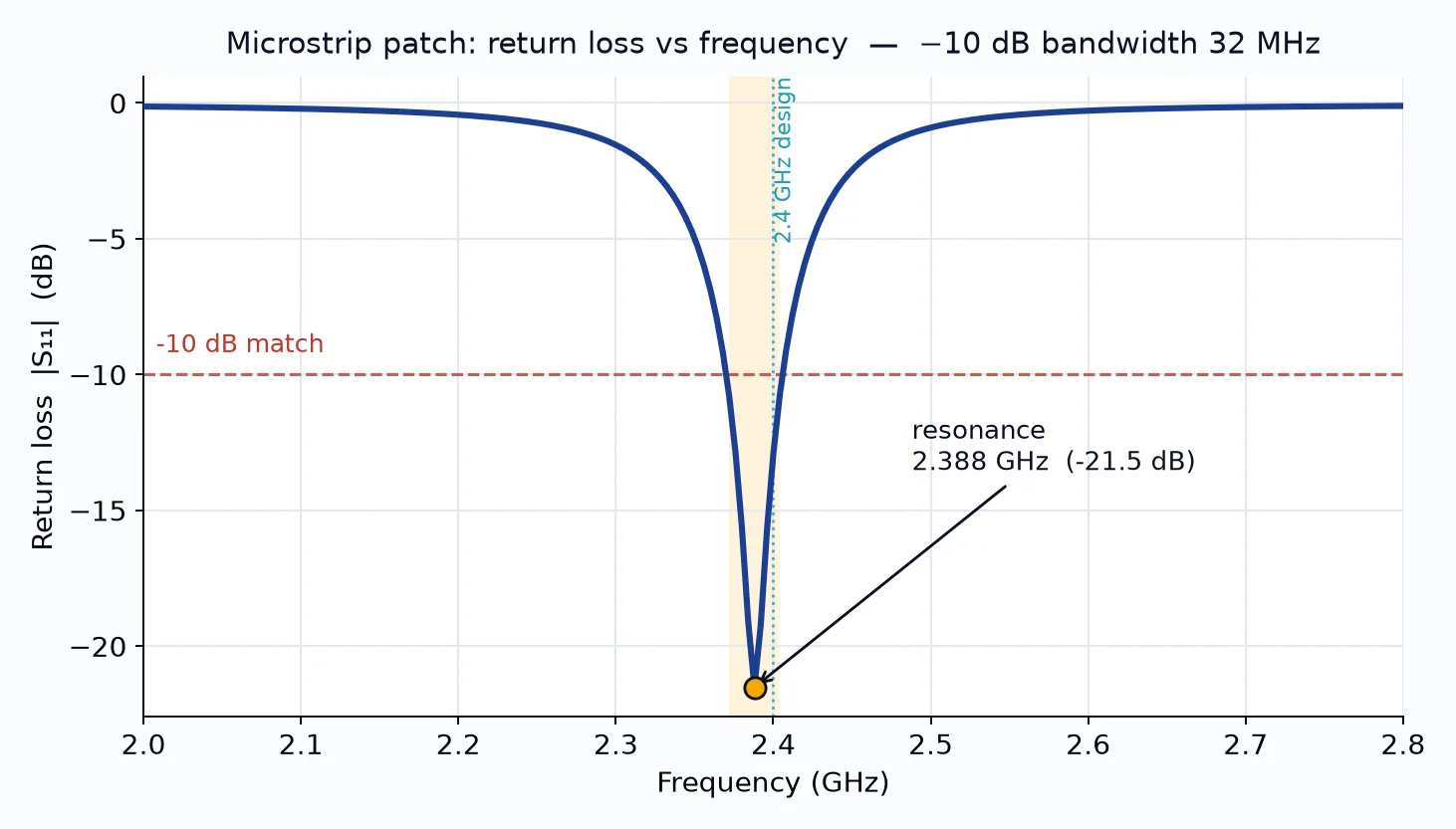
The credibility here is not the pretty lobe — it is that the lobe was predictable. The classic transmission-line model of a patch, a closed-form calculation you can do on paper, says: take half the guided wavelength in the substrate (here 43.0 mm), subtract a small correction for the fields that fringe past each open end, and that is your patch length — which lands the resonance at 2.400 GHz. HFSS, solving Maxwell’s equations on the actual geometry with no such assumptions, put it at 2.388 GHz. The two agree to 0.5% — about 12 MHz. The hand-calc gets you almost all the way; the full-wave solve captures the last half-percent of fringing and feed detail the formula rounds off.
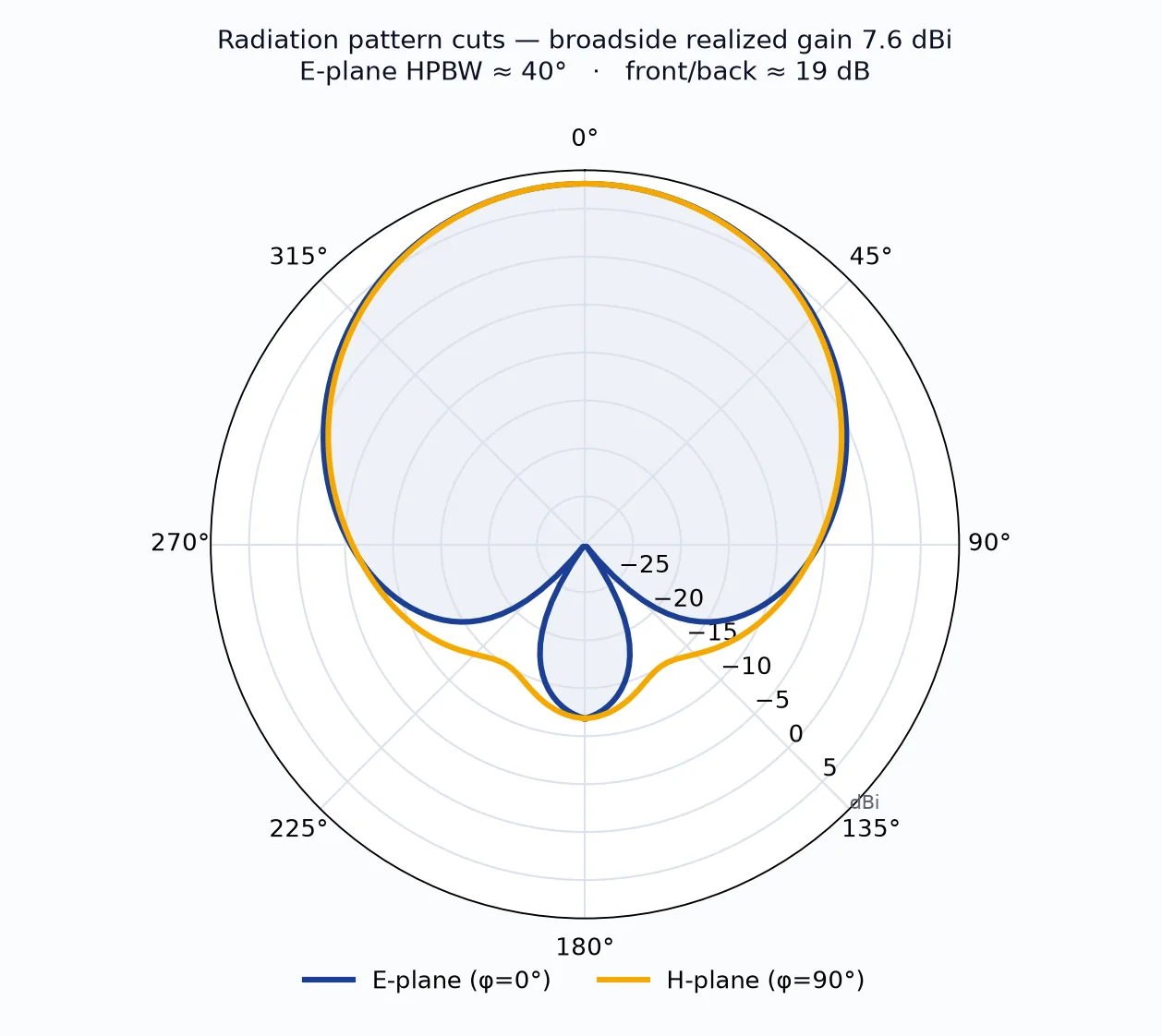
And it is not just the frequency. The 7.6 dBi gain lands slightly above the 6–7 dBi band textbooks quote for a half-wave patch — above it, not in it, and we say so: idealizing the copper as a perfect conductor accounts for only ~0.1 dB of the excess, and the rest belongs to this particular geometry rather than to the generic textbook case. What actually makes the gain trustworthy is a self-check the pattern itself provides. Pair the gain with the two solved beamwidths — 79° E-plane, 75° H-plane — and the classical beamwidth-product rule estimates a directivity of 41,253/(79 × 75) ≈ 7.0, or 8.4 dB: within a decibel of the solved 7.6 dBi, and high in exactly the direction that rough rule errs (it assumes all power stays in the main beam, ignoring the back lobe sitting ~19 dB down). A 40° beamwidth — the number an earlier version of this page printed — would demand roughly 4 dB more gain than the solver reports; 79° × 75° and 7.6 dBi belong together. Add the 1.3% bandwidth — exactly what a thin single-layer patch gives; patches are famously narrowband — and the study has three independent checks: frequency against the hand formula, gain against its own beamwidths, bandwidth against the patch's known character. That is the difference between a rendering and a simulation.
Why it matters: the half-wavelength rule is everywhere
2.4 GHz is the crowded downtown of the radio spectrum — Wi-Fi, Bluetooth, Zigbee, cordless everything, and, yes, your microwave oven all live in that band. The reason the antennas for it are flat little rectangles is the same half-wavelength rule we just watched play out: a patch has to be about half a guided wavelength long, and at 2.4 GHz on this board that is ~41 mm — matchbook-sized, easy to print. Drop to 900 MHz and the same patch grows to palm-sized; climb to a millimeter-wave 5G band and it shrinks to a grain of rice, which is exactly why phone makers can pack dozens of them into a steerable array. Change the frequency, the copper resizes itself; the physics is the ruler.
The same rule also says what this particular patch still needs before it could serve a real router. As solved, its −10 dB band (2.372–2.404 GHz) sits almost entirely below the 2.401–2.483 GHz Wi-Fi allocation — a 3 MHz overlap, no channel covered. Length sets frequency, so the fix is a trim: shortening the patch about 2% — from 41.3 to roughly 40.5 mm — scales the resonance from 2.388 to about 2.44 GHz, parking the band on the middle Wi-Fi channels. We report the model as it solved rather than nudging the numbers after the fact; the trim is the next design iteration, and the half-wavelength rule prices it at under a millimeter of copper.
That broadside beam matters just as much as the size. Because a patch aims its energy straight off the board, designers can lay it flat against the inside of a case, a car roof, a drone belly, or a satellite panel and know which way it will “look.” Tile a few dozen together, feed them with slightly shifted timing, and the combined beam can be steered electronically with no moving parts — the trick behind modern radar, 5G base stations, and Starlink terminals. It all starts with getting one rectangle to resonate at the right frequency and accept its power, which is precisely what the return-loss dip above confirms.
Need an antenna sized, matched, or its radiation pattern predicted before you commit to a board spin — on a phone, a wearable, a drone, a vehicle, or an implant? The same Ansys HFSS workflow — geometry, adaptive mesh, a matched port, and a full-wave solve checked against theory — is how simulation answers “where does it resonate, will it match, and which way does it radiate” before the first prototype exists. That’s innovation through insight.